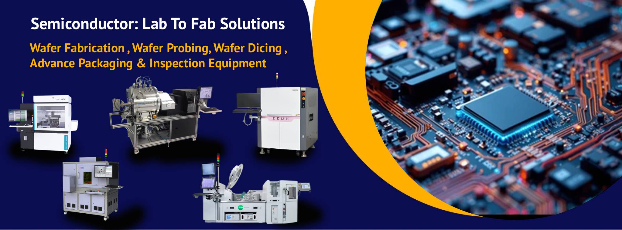
Wafer Fabrication , Wafer Probing, Wafer Dicing , Advance Packaging & Inspection Equipment Wafer Level test solution (MEMS)Environmental Sensor CalibrationApplication specific Wafer probing & final testMotion Sensor CalibrationCryogenic Wafer Prober Ion Beam DepositionIon beam DelayeringIon Beam EtchICM SputteringPE-CVD Plasma Enhanced Chemical Vapor DepositionMagnetron Sputtering (UBM)Planer cathodesPIB -CVD Plasma Ion Beam Assisted Chemical Vapor Deposition Production BondersR&D BondersRework Equipment Wafer Inspection systemWafer to wafer Die sorterCamera inspection SystemLens Sorter & Inspection system Manual probe stationAutomated Probe stationLaser Repair machine Laser Wafer Cutting SystemDual Head Strips Laser markerLaser – based package singulation system 3D Wafer Bump & Wire Bonding AOI Inspection systemWafer Bump 3D Vision Inspection Flip Chip Machines for Assembly of Facing Down Chips/DiesReballing/Deballing for Repairing of Defective Solder Balls on BGA3D Package Machines for Interconnecting Dies/Chips On WafersProbe Card Machines for Semiconductor Chips and ModulesWafer Level Packaging Services SEM(Tabletop SEM)X-Ray Inspection SystemSemiconductor Packaging Systems Inline 3D X-ray Inspection Machine for IGBT Power Modules Ultra Low Dry CabinetLow RH% Dry CabinetBaking 60 Dry Cabinet Automated Optical -wire bonding inspectionAOI & AXI Wire Bond InspectionInline 3D Xay for inspection