
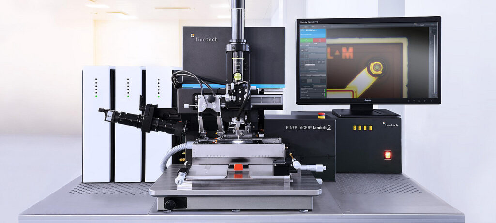
FINEPLACER® lambda 2
Descriptions
The ultimate tool for optical assemblies with 0.5 placement micron accuracy offering superior optical resolution and excellent price performance. The completely revised table top die bonding platform can be easily configured for a wide range of applications for process development or prototyping. Numerous process module options and in-field-retrofit capabilities guarantee maximum technological flexibility of the table top die bonder to protect your investment in the face of ever-changing challenges.
Feature
- Synchronized control of all process related parameters: force, temperature, time, process environment, illumination, vision
- Extended object field with optics shifting in x
- In-situ process observation in HD
- Overlay vision alignment system (VAS)with fixed beam splitter
- Data/media logging and reporting function
- Full process access and easy programming
- Proven software ergonomics
- Modular machine platform allows in-field retrofitting
Benefits
- Maximum process reproducibility
- Precise alignment of large components, relative placement capability
- Immediate visual process feedback
- Precise visual alignment of chip and substrate
- Comprehensive process documentation and traceability
- Fast and intuitive process implementation
- Easy to use for new operators
- Easy upgrade to meet new application & technology requirements
Technologies
- Adhesive bonding
- Sintering
- Soldering/eutectic soldering
- Thermocompression bonding
- Thermo- /ultrasonic bonding
Applications
- Acceleration sensor assembly
- Gas pressure sensor assembly
- Ink jet print head assembly
- Laser diode assembly
- Laser diode bar assembly
- MEMS
- MOEMS
- NFC device
- RF/HF module
- RFID module
- VCSEL/photo diode (array) assembly
- Image sensor assembly
- X-ray detector assembly
Processes
- Chip on Flex /Film (CoF)
- Chip on Glass (CoG)
- Flip chip bonding (face down)
- Precise die bonding (face up)
- Wafer level packaging (C2W)
- 2.5D and 3D IC packaging (stacking)
Modules & Options
- ACF Module
- Bonding Force (automatic)
- Bonding Force (manual)
- Chip Heating Module
- Component Presentation
- Die Eject Module
- Die Flip Module
- Dipping/Stamping Module
- Direct Component Printing Module
- Dispense Module
- Flip Chip Test Module
- Formic Acid Module
- Mask Generator
- Optics Shifting
- Process Gas Module
- Process Video Module
- Reballing Module
- Scrubbing Module
- Substrate Heating Module
- Substrate Support
- Target Finder
- Ultrasonic Module
- UV Curing Module
- Wafer Heating Module
- Zoom Optics